PCB Manufacturing
As hobbyists ourselves, we organize local mfg power, panelize designs, reduce the shipping cost, and ensure the quality. It will be a source to sustain our company along with other services we provide. The minimum PCB quantity we accept for mass production is as low as 10 pieces. When you order PCB through our online system, we will send you a confirmation with an order number. To make sure orders processed smooth and accurately, mark your order number in silkscreen layer, pack Gerber files into a zip file named A[order number]_[PCB size] (example: A14756_10X10.rar) and then email to sales@lankapcb.com by including order number in the subject line. Please be sure to avoid boards less than 2cm to reduce cost. If the file and design meet the LankaPCB guidelines, they will be processed and shipped in 1 to 2 weeks based on the order quantity.
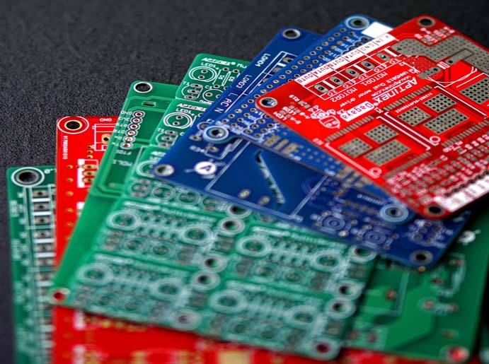
Gerber file requirement
The following layers are needed
- Top layer: pcbname.GTL
- Bottom layer: pcbname.GBL
- Silk Top: pcbname.GTO
- NC Drill: pcbname.TXT
- Solder Stop Mask top: pcbname.GTS
- Solder Stop Mask Bottom: pcbname.GBS
- Silk Bottom: pcbname.GBO
Note: Board outline must be included at least in one layer.The Gerber file must be RS-274x format.
Quality
- Your Gerber file must include only one design
- Drills line and long slot can’t be accepted
- Minimum slot 1mm*1mm
- DRC compatible as rule file attached
- The PCB size is smallest rectangle that can accommodate PCB
Clarification to panelizing
For the service
- 5cm Max * 5cm Max
- 10cm Max * 10cm Max
- 10cm Max * 15cm Max
- 5cm Max * 10cm Max
- 5cm Max * 15cm Max
you can panelize to save the cost. However you are required to cut the boards by yourself or get it done by us for a nominal fee.
The rules of panelizing
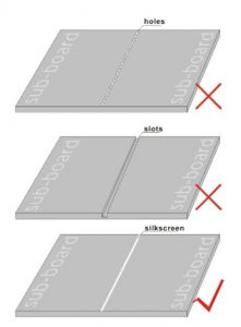
- There should be no more than 5 sub-boards to fit the size.
- The sub-boards should only be separated by the silkscreen.
Using Any holes or slots to separate the sub-boards are not permitted.
Available quantity option
We undertake any order in multiples of 10.
Note: If you want to order more than 10 pcs, please do check the price for different options and find the most economic one.
LankaPCB PCB capabilities
- Multi Layers: 1-2
- PCB Material: FR-4
- Available Color: Green, Red, Yellow, Blue and White. We provide Green free and the rest for an additional cost.
- Silk Screen: White, Black (For White Solder Mask only)
Available board thickness
0.8mm, 1.0mm, 1.2mm, 1.6mm, 2.0mm
- Thickness Tolerance: (t=0.8mm) ± 10%
- Thickness Tolerance: (t<0.8mm) ± 10%
- Insulation Layer Thickness: 0.075mm–5.00mm
- Minimum trace width: 6mil (6/1000 inch);
- Minimum trace/vias/pads space : 6mil (6/1000 inch);
- Minimum silkscreen width : 4mil (4/1000 inch)
- Minimum silkscreen text size : 32mil (32/1000 inch)
- Out Layer Copper Thickness: 1oz (35um)
- Inner Layer Copper Thickness: 17um—100um
- Drilling Hole (Mechanical): 0.3mm—6.35mm
- Finish Hole (Mechanical): 0.3mm—6.30mm
- Diameter Tolerance (Mechanical): 0.08mm
- Registration (Mechanical): 0.09mm
- Aspect Ratio 8:1
- Solder Mask Type: Photosensitive ink
- SMT min Solder Mask Width: 0.1mm
- Min Solder Mask Clearance: 0.1mm
- Plug Hole Diameter: 0.25—0.60mm
- Surface Finish: HASL, HASL (Lead Free) +$5, ENIG+$10.
Available maximum size
- 50mm X 50mm
- 50mm X 200mm
- 100mm X 200mm
- 200mm X 200mm
- 50mm X 100mm
- 100mm X 100mm
- 150mm X 150mm
- 50mm X 150mm
- 100mm X 150mm
- 150mm X 200mm
Note: The PCB maximum dimensions for each price bracket are just that, the maximum. Your PCB design must be smaller than the dimensions of the service you select.
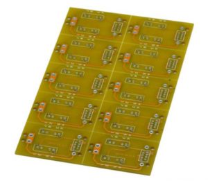
Available E-TEST options
50% e-test, 100% e-test
Note: Tested PCB will have a mark on the PCB edge.
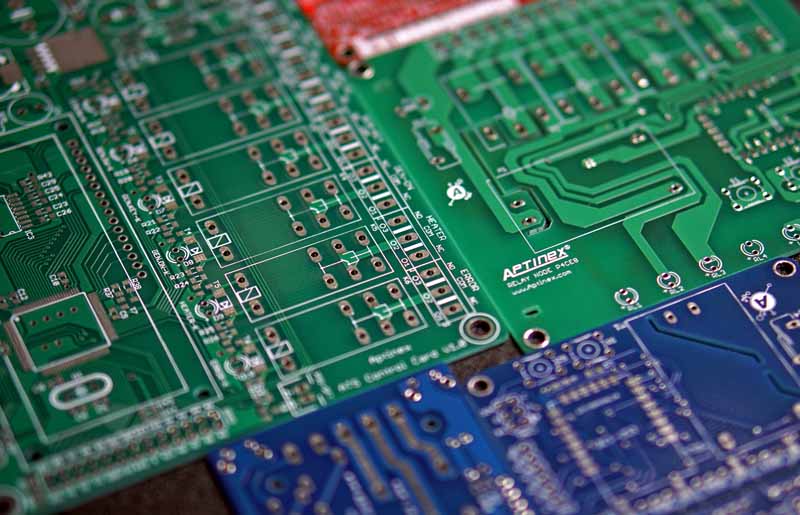
Surface options
HASL (Hot Air Solder Leveling)

The most common surface finish that you can see on PCBs. HASL boards are dipped in molten solder and then the excess is cleaned off using hot-air knives to leave behind the thinnest possible layer of solder. Afterwards the solder itself protects the underlying track from corrosion while making it extremely easy to solder on parts. This is because the whole pad is pre-tinned. Generally considering, this is the cheapest finish available and probably a great choice for general-purpose boards.
One downside to HASL is that even after the hot-air knife has cleaned off as much excess as possible, the meniscus of the solder will still cause the edges of pads to be slightly rounded. That makes surface-mount parts not sit down quite as flat as they would on an ENIG board.
ENIG (Electroless Nickel Immersion Gold)

ENIG Boards consists of an underlying layer of nickel with a thin layer of gold over the top. However the gold layer is very thin and not intended to provide the main structure of the track, it just acts as a protective coating for the nickel to prevent it tarnishing before it’s soldered. Gold is extremely resistant to corrosion so ENIG has several good points: it can be touched with bare fingers without tarnishing, has a very long shelf life, and the pads / tracks are very flat and square-edged – something that can be important for fine-pitch surface-mount parts.
One bad aspect to ENIG though is that it takes a bit more solder to complete a joint because the surface hasn’t yet been pre-tinned, and because there isn’t an existing layer of solder to melt against the iron and increase the initial contact area (hence increasing the rate of heat transfer) it can take an extra second or so to get the joint hot. You really need to make sure your iron has good contact with the joint to make sure enough heat is transferred to the track and the component lead.
