How to export KiCad-5.1.5 PCB to Gerber files and NC Drill file
Generating Gerber Files
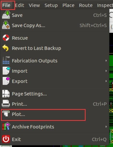
- Select File -> Plot from the menu to open the Gerber generation tool.
- At the top of the pop-up window, you’ll see the folder location for your files, click browse. Make sure you’re in your project directory.
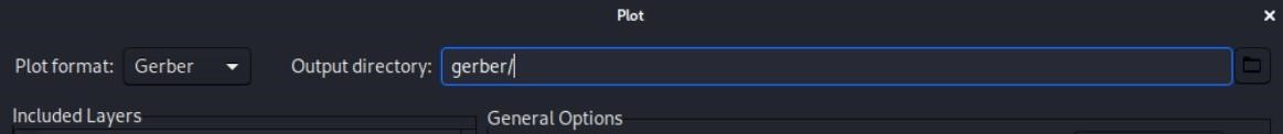
- Make a new folder called Gerbers, select it and click select folder. Click yes if asked to use a relative path. On the left side, you’ll see which layers from our board design we want to turn into Gerber files.
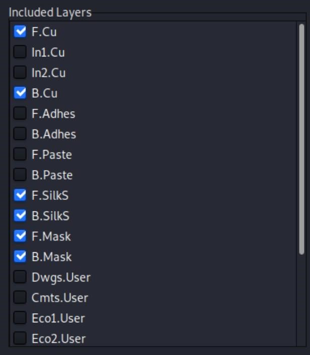
- Select all the layers you need. For a simple PCB, you’ll need the
- Top and Bottom silkscreen layers
- Front and back copper
- Edge cuts
- The In1 and In2 layers are only needed for four-layer boards.
- Make sure the front and back copper layers are checked as well as the front and back silkscreen layers. Check the front mask, back mask, and edge cuts.
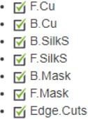
- The mask layers show where the solder mask needs to go and the edge cut layer is our board outline with the slot cut out at the top. It also gives us which options we need to check.
- Make sure that the “Exclude PCB edge layer from other layers” is checked. We want the part reference designators to show up on the board so leave that checked. But we don’t want the values to be printed, so uncheck “Plot footprint values”.
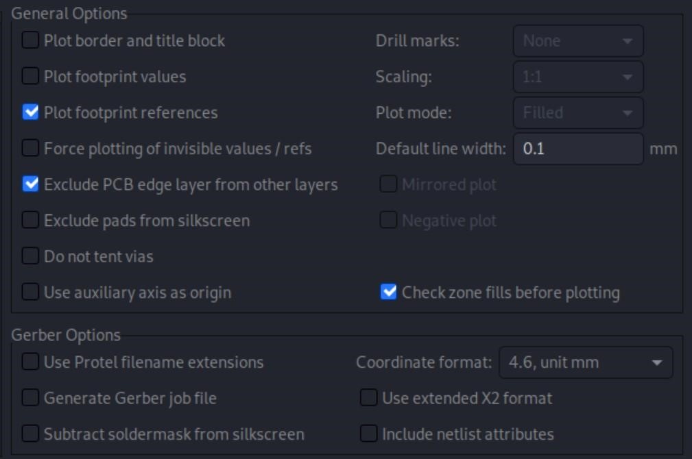
- Click “Plot
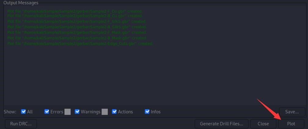
- Gerber files will be generated and saved in the Gerbers folder.
Generating Drill file
- Check the below options and leave everything else to default.
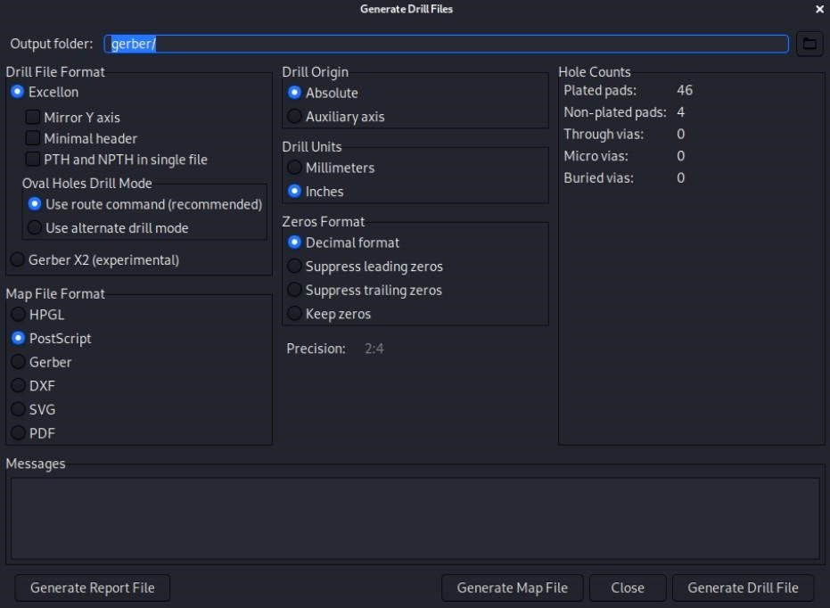
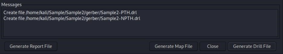
- Click “Generate Drill File” and you should see a message in the bottom text window indicating that new files were created.
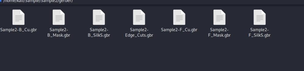
Verify the Files
Next, click “Close” to exit the Generate Drill File windows. All of the files should have appeared in your gerbers folder. Then select all of the files and zip them up.